The Internet has many articles on how to create new Fritzing parts. But, unfortunately, it is often a lot of text and is overlooked nekoorye the key points of creating an SVG file. I'll Write the version of manufacturing fritzing part from scratch on the items on the free SOFTWARE. To work you need to:
- Fritzing Application for drawing diagrams and PCB.
- Templates and fonts for fritzing parts.
- Inkscape for rendering vector SVG files.
- Paint.net for photo editing.

In The example, I will create a fritzing part for the SIM800C module.
Layout Board
To Create a layout board, you must:
- Find a snapshot of the module from above. A Suitable frame can be found either in the Online store, or make the frame yourself. I found the right frame here.
- In Paint.Net I turn the photo so that the board was strictly horizontal. Trusted on-0.2 oC
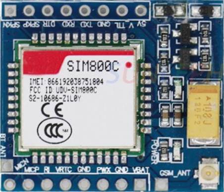

- I Measure the exact size of the board: 31 mm x 26.5 mm. Holes for pins are absent on 1.5 mm on top and 1.5 mm on the side.
- I Open Inkscape. And in the File-> Document properties… menu. Indicate Display units-> mm and Units-> MM.
- The Size of the sheet is exhibited in the size of the board: 31 mm x 26.5 mm.
- I'm moving to Grids. I Change Units-> MM. Create a new Grid with increments of 0.1 "or 2.54 mm. Spacing X and Spacing Y-2.54 mm. 0.1 "-A typical step of holes in the breadboard.
- Insert an image in Inkscape.
- Right-click on the image and select the Object-> Transform menu item.
- I'll move to the Scale tab.
- I Put a galku near Scale proportionally for proportional scaling of the image.
- Choose units-> MM.
- I set the width to 31 mm. The Height is automatically recalculated and displayed-26.6. Lucky, the photo on the scale and the camera is done well.
- Choose Apply to accept the changes.
- I Disable sticking to the grid ("Snap to Grids") in the right menu. I Circled the screenshot in red.
- I place a scaled image GJ wtynhe the kbcnf of the sheet.
- Unpack the archive with templates and open the file PCBViewGraphic_Template. svg from the Templates folder. From This file we need contact areas. Copy to our file with the card SIM800C.
- On the border of the board image draw a rectangle in the size of the board 31 mm x 26.5 mm. Holding down the ALT key and the cursor keys accurately adjust the rectangle so that it goes exactly on the circuit board.
- Open File-> Document properties… -> Grids and select Origin X and Origin Y so that the mesh node begins strictly from the center of the first top hole. Taking into account the standard of pin placement through 0.1, the "mesh nodes shall be at the center of each pin of the upper comb.
- Check the instruction "Measurement tool (M)" that the distance to the first output of the comb side and top is about 1.5 mm.
- Copy the contact pad taken from the template, on top of all the pins of the comb, so that the mesh knot coincides with the center of the contact pad.
- Using the Align and distribute Objects tool (Shift + Ctrl + A), align the contact pads in the middle (Align-> Center on horizontal axis) and align the distance between the platforms horizontally (Distribute-> Distribute centers equidinstantly Horizontally).
- Select all the contact points of the top comb by holding down Shift and then grouping, pressing the right mouse button and selecting Group in the drop-down menu.
- I Copy grouped conclusions and I shift to the bottom comb. Unfortunately the distance between the combs in the board SIM800C made not multiple 2.54 mm, ie The breadboard will not stand up. Accordingly, the horizontal grid line at the bottom will not coincide with the centers of the bottom comb pins. Therefore Add a Guide (Guid), placing the cursor on the top ruler (under the menu), holding the left mouse button and dragging, without releasing the key, to the bottom comb. I release the mouse button in the right place.
- The Contact pads for both combs have been added. The Most important point is to rename their ID, otherwise Fritzing after importing the SVG file will not accept the added sites as PINS. The correct PIN name, for example, is Connector7pin. You can only Change the digit. If you add any other symbol at the end of the title (after pin), Fritzing will not accept the contact pad.
- Open the Object Properties dialog box (Shift + Ctrl + O).
- While Holding Ctrl, select the contact pads in the grouped block of the top comb and rename the ID to be: Connectorpin,[номер] and Label-#connector[номер]pin.
- The same operation is done with the bottom comb.
- Using Graphical primitives (rectangles, circles) draw on top of the electronic elements of the board their image. It takes literally 15-20 minutes.
- When Selecting colors, you can use the Color Picker tool in Paint.Net. After that the color code in HEX is copied to Inscape to paint the corresponding element. Naturally, you can not complicate and use similar colors from the bottom palette of colors Inkscape (Shift-Alt-P).
- From the archive with templates and fonts install fonts.
- I put the inscription on the board with a DroidSasns font of white color, selecting the appropriate font size.
- Unfortunately, Fritzing after importing SVG files ignores the font size. To Make the Srif unchanged, it must be converted to curves.
- Before you convert to curves, you can add a separate layer Text to copy the original version of the text, in case you need to fix something. You must disable the Display of the text layer.
- I select All labels with hold Shift and then in the menu Path-> Object to Path (Shift-Ctrl-C).
- Unfortunately, Fritzing does not display or display with errors The board image, so hide it by creating a layer named Image. Select the image and in the right-click menu choose Move to Layer… by specifying the Image layer to move.
- The SVG file is ready to create a new Fritzing part. In Fritzing, choose any of the part-S and right-click. Choose the menu item Edit part (new parts Editor…).

- In The opened editor Kompronentov select the bookmark Breadboard, then in the menu File-> Load image to view… Choose the SVG file you created.
- A drawn SVG file appears on the Breadboard tab. After making sure that the image is OK and all the pins are properly imported, you need to associate pins with PIN names.
- For The PIN association, it is allocated in the Connector List, if it is necessary to change its name and description, and then click on the button that appears near the output, Select graphic, and then select the PIN to be associated with the corresponding Leg.
- After the association to the left of the name pin-A will appear a jackdaw.
- If you see fewer pins on the right than on the board, you can add more on the Connections tab by specifying the total number or manually adding the required pins.
Concept
To Create a printer module diagram:
- Open the SchematicViewGraphic_Template. svg template
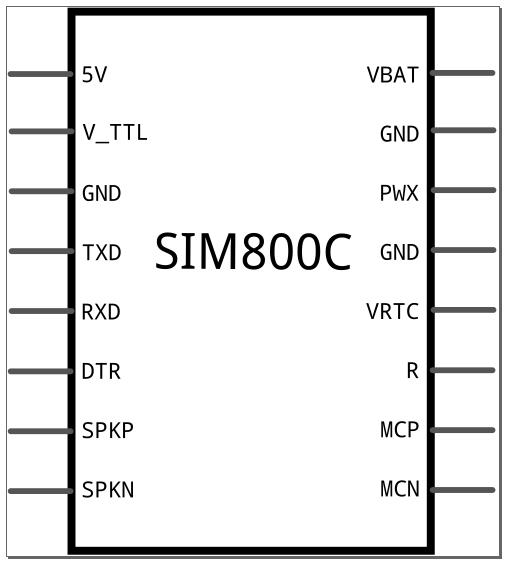
- The module has only 16 legs.
- Ungroup the template.
- Delete superfluous inscriptions and elements.
- I Copy the necessary number of pins, reconciling the distance between them.
- Align the vertical conclusions (Distribute-> Distribute centers equidinstantly vertically) and contours (Align left edges) using the corresponding tools Align and Distribute objects (Shift + Ctrl + A).
- I Increase the size of the scheme rectangle so that all the conclusions are cleared.
- The 8 pins Created on the left after alignment are grouped and copied for transfer to the right side.
- I put the inscriptions in the font Droid Sans C Font Size-2.
- I'Ll Rule the central inscription on SIM800C.
- Unfortunately, fritzing often changes the size Of fonts after import. If This is the case, I use the font translation in the curves as a workaround. To do this, I highlight all the inscriptions and translate into curves:
Ctrl +K (path combine), thenCtrl +J (dynamic offset)- The text Color should be changed to white, otherwise in the PCB the letters can be displayed very greasy.
- I Change the size of the sheet so that the resulting image is only slightly smaller than it.
- I go to Fritzing on the Schematic tab and Load the sothe SVG file through the file-. (Ctrl-O).
- For the Association of pins on the drawn Prinitpiličesya scheme with already available connections choose the desired pin in the Connector List.
- If you need to change its name and description.
- Click on the pin that appears near the name and Select graphic, and then highlight the pin that should be associated with the corresponding leg.
- After the association to the left of the name pin-A will appear a jackdaw.
- Next you need to specify in the section "Terminal Point" where the connection line will be attached: Center, W (EST), E (AST), S (Outh), N (Orth). Accordingly, for the legs to the left of the rectangle for all pins should be set W (EST), and for all right-E (AST). The Cross on the connection line moves, respectively, to the left or to the right.

- Save parts by selecting the Fle—.
Pcb
The SVG file is obtained from Breadboard. To do this:
- I save the SVG file by replacing the breadboard suffix with the PCB.
- Mirror the breadboard relative to the comb pins.
- I'm Transferring all the inscriptions to the conclusions.
- Remove all unnecessary elements, leaving only the contact areas, the border of the board and text.
- The distance between the comb peaks is Thoroughly extinct. I Got 24 mm.
- The Two lines of the child are placed so that the distance between them is strictly 24 mm.
- Align the combs with the board using Align and Distribute (Shift + Ctrl + A) so that they are symmetrical with respect to the board. In Breadbord It was possible to place contact platforms on a photo, in the case of a printed circuit board on a photo it is impossible to pay attention, only exact sizes.

- The combs are grouping. In Object Properties (Shift + Ctrl + O), I specify ID: Copper0, Label: #copper0.
- The Text and the frame of the board group and specify the ID: silkscreen, Label: #silkscreen.
- Just In case I select the group COPPER0 and execute the command "Raise selection to Top" to move on top of all the elements. If You do not, you will not be able to select separate pins for connections binding after importing the PCB into ftitzing.
- Save.
- In Fritzing, I move to the PCB tab and load the created file.
- I Bind to the contact areas of the connection.
- Save.
Icon
There is no need to create a SVG file Specifically for an icon. It is Enough to load a previously created breadboard SVG file.
On The Icon tab, go to the menu File-> Load image to view… Choose the SVG file previously used for Breadboard to be displayed as an icon in the part-S palette in fritzing.
I Save the created Fritzing part: File-> Saved (Ctrl-S) and specify the name SIM800C.
Fritzing part for SIM800C
After you have loaded all the components to create a fritzing part for SIM800C, you need to create a *. fzpz file. To do this:
- Creating a new project Fritzing.
- I Find the SIM800C component in the fritzing parts on the right.
- Right-click on the SIM800C icon and select Export part….
- I save a file named SIM800C. Fzpz.
- And that's all. The Final file is here.
Useful notes
To not edit the text, I will add finds to this section.
Silkscreen
Labels, circuit boards, and any other elements that need to be displayed in the PCB must be grouped with the name silkscreen.
Often the text after import into fritzing is deformed. For example, the position is correct, but the font size becomes different.
Above I have already written that in order to save the font it needs to be converted into curves. The Problem is that with this conversion the font becomes not editable and if there is an error in it, you have to re-type the text and then re-enter the curves.
To not type text and other objects every time, I recommend that you create multiple layers in Inkscape:
- The Text Layer in which the source text will be saved, so that it can be taken in the case of editing. This layer needs to be hidden.
- The image Layer in which there is a photo of the card of the module or some element on top of which the vector image of the board will be drawn. The Layer should be located at the bottom. This layer should be hidden Before saving the finished SVG file.
- The Copper Layer in which all the contact areas are located. The Elements in it will need to be grouped and named group Copper0.
- The Silkscreen Layer, which will contain all the elements that should be displayed in the PCB Image: circuit board, text converted to curves. The Objects in this layer should be grouped and given a name to the silkscreen group.
Converting text to curves for PCB
To convert Text to curves:
-
Ctrl +K (path combine) Ctrl +J (dynamic offset)- The text Color should be changed to white, otherwise in the PCB the letters can be displayed very greasy.
Extracting *. svg files from *. fzpz
In Some cases it is useful to take some components from *. svg files made by colleagues. However, often there is only a ready *. fzpz file with fritzing parts.
In some cases, the export of *. svg file from the editor Parts Editor occurs with errors. This happens, for example, in the case of large files.
Fzpz file fritzing Parts is a regular zip archive in which all the necessary *. svg files are separately. So It's easy to borrow. 🙂